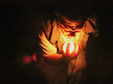
We’ve updated our Terms of Use to reflect our new entity name and address. You can review the changes here.
We’ve updated our Terms of Use. You can review the changes here.

Electrochemical, photoresistive and photomagnetic properties of semiconductors

by ewa justka

/
  • Streaming + Download

    Includes unlimited streaming via the free Bandcamp app, plus high-quality download in MP3, FLAC and more.
    Purchasable with gift card

      £7 GBP  or more


1.
2.
3.
4.
galena 00:51

about

A semiconductor is a material which has electrical conductivity between that of a conductor such as copper and that of an insulator such as glass. Semiconductors are the foundation of modern electronics, including transistors, solar cells, light-emitting diodes (LEDs), quantum dots and digital and analog integrated circuits. The modern understanding of the properties of a semiconductor relies on quantum physics to explain the movement of electrons and holes inside a lattice. An increased knowledge of semiconductor materials and fabrication processes has made possible continuing increases in the complexity and speed of integrated semiconductor devices, an effect known as Moore's Law.

The electrical conductivity of a semiconductor material increases with increasing temperature, which is behaviour opposite to that of a metal. Semiconductor devices can display a range of useful properties such as passing current more easily in one direction than the other, showing variable resistance, and sensitivity to light or heat. Because the electrical properties of a semiconductor material can be modified by controlled addition of impurities, or by the application of electrical fields or light, devices made from semiconductors can be used for amplification, switching, and energy conversion.

Current conduction in a semiconductor occurs through the movement of free electrons and "holes", collectively known as charge carriers. Adding impurity atoms to a semiconducting material, known as "doping", greatly increases the number of charge carriers within it. When a doped semiconductor contains mostly free holes it is called "p-type", and when it contains mostly free electrons it is known as "n-type". The semiconductor materials used in electronic devices are doped under precise conditions to control the location and concentration of p- and n-type dopants. A single semiconductor crystal can have many p- and n-type regions; the p–n junctions between these regions are responsible for the useful electronic behaviour.

Some of the properties of semiconductor materials were observed throughout the mid 19th and first decades of the 20th century. Development of quantum physics in turn allowed the development of the transistor in 1948. Although some pure elements and many compounds display semiconductor properties, silicon, germanium, and compounds of gallium are the most widely used in electronic devices.

(en.wikipedia.org/wiki/Semiconductor )

credits

released July 29, 2014

license

all rights reserved

tags

about

ewajustka

handmade synthesisers & contingent rabbit holes

contact / help

Contact ewajustka

Streaming and
Download help

Report this album or account

If you like Electrochemical, photoresistive and photomagnetic properties of semiconductors, you may also like: